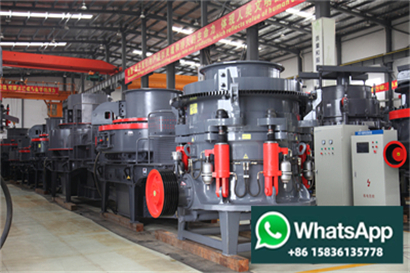
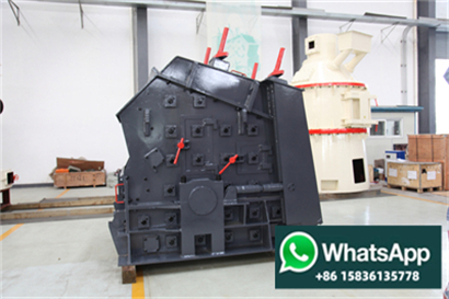
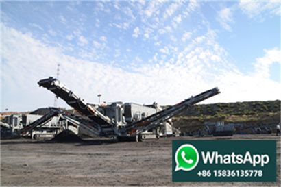
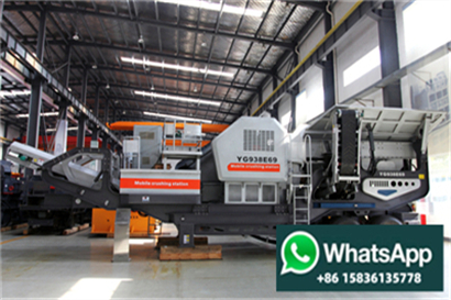
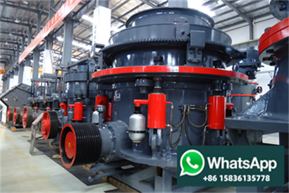
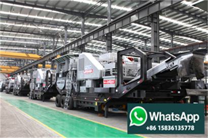
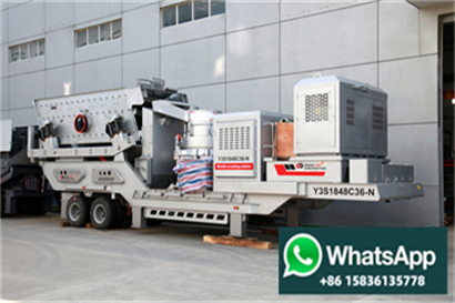
كسارة الحجر المتنقلة هي حل معياري أكثر شمولاً ومنهجية ومرونة تقدمه الشركة للعملاء. وهي مجهزة بمعدات مضيفة مخصصة عالية الأداء، مع حجم صغير وقوة معالجة قوية؛ يعتمد الإطار على تصميم شعاع مستقيم بسيط ومجهز بدعائم ثابتة قابلة للتعديل. يتمتع الإطار بثبات جيد ويمكن تركيبه ونقله بسرعة عدد كبير من السيور الناقلة المركبة لديها اتصال ونقل أكثر معقولية وموثوقية، ويمكن تركيبها واستخدامها بسرعة، ويتم اعتماد نظام التحكم الكهربائي المتكامل لضمان التشغيل الفعال والمستقر لخط الإنتاج.

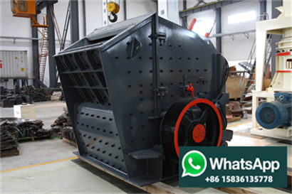
تلتزم الشركة دائمًا بمعدات سحق التعدين ومعدات صنع الرمل ومعدات الطحن الصناعية، وتوفير حلول عالية الجودة للرمل والحصى ومجموعات كاملة من المعدات للمشاريع الهندسية واسعة النطاق مثل الطرق السريعة والسكك الحديدية والمياه والكهرباء، إلخ. ، وتسعى جاهدة لممارسة التصنيع الدقيق المحلي والتخطيط العلمي العالمي، مع اعتبار آسيا المنطقة النائية والعملاء المشعين حول العالم. بعد أكثر من 30 عامًا من التطوير، نجحت العديد من منتجات الشركة في اجتياز العديد من شهادات الجودة الدولية مثل الشهادة الدولية ISO9001:2015، وشهادة الاتحاد الأوروبي CE، وشهادة GOST الروسية. بعد ذلك، في السعي لتحقيق التميز، سنستمر في استخدام منتجات عالية الجودة والتكنولوجيا الاحترافية والخدمات المخلصة لمساعدة العملاء على خلق قيمة أكبر، واستخدام الإجراءات العملية لمواصلة تعزيز البناء البيئي للحضارة الإنسانية.


6 ·Following the nickel plating immersion gold deposition produces the thin protective gold overlayer The PCB panel is simply immersed in an acidic immersion gold plating solution containing a gold salt The gold ions undergo galvanic exchange with nickel atoms to spontaneously deposit a thin gold layer around μm thickness No
·PCB Gold fingers are specialized gold plated columns located along the edges of printed circuit boards PCBs For example in auto assembly lines or food packaging plants gold finger equipped circuit boards enable the seamless execution of commands by computer controlled machinery Gold fingers are employed in various ways
·The Pros and Cons of Immersion Gold Plating vs Gold Plating for PCBs In the realm of printed circuit board PCB manufacturing surface finish plays a pivotal role in determining the board s performance durability and cost effectiveness
4 ·Gold plating Later to mil of hard gold is plated over the nickel The gold is usually mixed with cobalt for increasing the surface resistance Edge beveling Edge beveling is a process of creating a transitional edge between two faces of a circuit board generally performed on the outer edge of the board Beveling allows for
·Gold plating kit is frequently used for printed circuits boards PCBs Since gold has strong conductivity good oxidation resistance and long life it is highly useful for the surface treatment of PCB boards The gold plating process involves depositing a thin layer of gold onto another metal through chemical or electrochemical plating This thin layer of gold is typically in
·PCB gold fingers also known as edge fingers are gold plated columns located at the edge of a circuit board Their primary function is to facilitate communication between different circuit boards When the power is on current flows along these metal contacts from one board to another enabling the transmission of digital signals
Vias are the conduits that allow electronic signals to pass between the layers of a PCB Oftentimes manufacturers add a layer of a conductive metal — typically copper — to a PCB s substrate to connect the board s layers as the necessary layout and holes are made For some applications copper plating is sufficient
·Gold plating provides a highly conductive corrosion resistant surface finish for printed circuit boards However thick gold plating is expensive so PCB designers must use it judiciously This article examines how thick gold can be plated on a PCB based on process limitations reliability factors use cases and cost considerations
·How thick is the ENIG Plating on PCBs The nickel layer is usually between 4 to 7 μm thick while the gold layer is a slender μm How does ENIG Plating Compare with Hard Gold Plating ENIG and hard gold plating differ in several ways including the method of gold attachment thickness cost and suitability for soldering
5 ·PCBs or Printed Circuit Boards are an essential component of almost every electronic device from smartphones and laptops to industrial equipment The plating of PCBs is an essential process that involves coating the circuit board with a conductive layer of metal to ensure proper electrical conductivity PCB plating is a critical step in the manufacturing process of these
Gold Plating Services presents the newest innovation in a turn key Printed Circuit Board gold plating repair kit for bench top brush plating and fine select gold plating This gold plating kit includes everything needed for fine select pen plating and brush plating 24K gold onto electronic and most other small parts The gold solution included
·Breadboard PCB for any type Raspberry Pi GPIO Gold plated finish prevents oxidation High quality Gold finish for easy soldering All holes are through plated for spacing ; 5PCS Mini Gold Plated Finish Solder able Breadboard PCB Diy Kit Packed with the high quality box
PCB Gold Finger Beveling On a circuit board the PCB gold finger plating process is used after the solder mask and before the surface finish The plating process generally consists of the following steps Nickel plating Between three and six microns of nickel are plated first to the connector edges of the fingers

·Besides the gold plated layer of WPCB was analyzed by X ray diffraction spectrometry XRD Ultima IV Rigaku Corporation Japan and X ray photoelectron spectroscopy XPS Thermo ESCALAB 250XI Thermo Fisher Corporation Download Download high res image 399KB Download Download full size image; Fig 2 Gold coated areas of a PCB from
·In the PCB manufacturing process into a multi layer circuit boards many customers will choose to use immersion gold or gold plated process but the specific immersion gold or gold plated customers are not very clear we are now sinking gold and gilded detail a difference as well as their advantages Immersion Gold is by chemical oxidation
1 Gold thickness in immersion gold board is more than that in a gold plating board Immersion gold board is more yellow than a gold plating board that because gold plating board has the color of nickel 2 Their crystal structures are different Comparatively speaking immersion gold is easier to be soldered with less poor solder issues
·This comprehensive guide delves into the world of PCB plating exploring its types processes benefits and considerations Understanding PCB Plating PCB plating is a sophisticated process that enhances the board s electrical and mechanical properties It involves the application of a thin metal layer over the base material or copper traces
EPLZON Solderable Breadboard Mini PCB Board Gold Plated Solder Breadboard for DIY Electronics Projects Apply to Soldering Projects "" Mixed Color Pack of 10 Pcs Blue 1 offer from $1199 $ 11 99 ELEGOO 32 Pcs Double Sided PCB Board Prototype Kit for DIY Soldering with 5 Sizes Compatible with Arduino Kits
5 ·On the other hand gold plating forms a hard gold layer that is abrasion resistant Other differences include the following What s the Difference Between Hard Gold and Soft Gold Plating on a PCB Board Gold plating involves electroplating gold on the copper pads However the precious metal cannot react with copper ions directly
·What are Gold Plated Boards Gold Plated Boards represent another significant category in PCB surface finishes Known for their robustness and exceptional conductivity these boards play a crucial role in high end electronic applications This section delves into the advantages and unique properties of Gold Plated PCBs 1 The Gold Plating Process
حقوق النشر © 2024 الشركة المصنعة لكسارة الصين